Technical / Research - Page 49

DisplayMate - the iPhone 5 LCD display is superior to the S3 AMOLED

Update: I just talked to DisplayMate's Raymond Soneira, and he says that the power-consumption test was done on an all-white screen. This is the worst-case scenario for an OLED, and so real-world results will be better (depending on your typical phone usage of course). 

DisplayMate posted an interesting and comprehensive comparison between the iphone 5 IPS-LCD and the Super AMOLED HD display used in the Galaxy S3. They say that the iPhone's display is superior - its a very accurate display, and it's the best Smartphone display they have ever seen. It's actually quite an improvement over the display used in the iPhone 4S.

DisplayMate says that the OLED display on the S3 is not as bright as the LCD, it is less readable in high ambient lighting, it has saturated green and distorted and exaggerated colors. They still complain about Samsung not calibrating the color gamut. On the other hand, they say that OLED is a new technology and hasn't been refined to the same degree as LCDs yet. They still say OLEDs have a very promising future.

Read the full story Posted: Sep 25,2012 - 8 comments

Researchers develop a CNT based flexible display TFT array

Researchers from Japan developed a new flexible display TFT based on carbon nanotubes (CNT), using a flexographic printing technology in ambient temperature and pressure. The carrier mobility is as high as 112cm2/Vs. The flexographic technology, while lower in precision compared to gravure printing, has a high throughput - much higher than screen printing or ink-jet printing.

The researchers used silver (Ag) nanoparticles for gate electrodes and source/drain electrodes, imide resin for gate dielectric films and CNTs for the channel layer of the TFT. Oxygen plasma is used for the CNT patterning and a printing technology is used to form a resist layer for it.

Read the full story Posted: Sep 19,2012

Sumitomo to join the Holst Centre's flexible OLED lighting research

Sumitomo Chemical has joined the Holst Centre's shared research program on Printed Organic Lighting and Signage. The program's aim is to develop new manufacturing processes that enable low-cost flexible OLEDs. Sumitomo will help the program's investigation of multi-layer solution processes for high-efficiency OLEDs, using the company's PLED materials.

Flexible OLED lighting prototype

Sumitomo will provide other program members access to its OLED materials - especially the emitting materials. Sumitomo will be able to use the program's expertise in order to optimize its own materials for low-cost production and flexible substrates.

Read the full story Posted: Sep 19,2012

The NEMO project concludes, new soluble OLED materials developed

The three-year long NEMO (NEw Materials for OLEDs from solutions) project has been successfully concluded. Merck, the project's leader, says that the new soluble materials developed in the project can now be used in large-area OLED display and lighting panels. The new phosphorescent materials have an increased lifetime (200,000 hours for green) and efficiency (70 cd/A @ 1,000 cd/m2).

NEMO was a large €29 million project, co-funded by the German Federal Ministry of Education and Research (BMBF). The project's scope included emitter materials, charge transport materials and new adhesives for reliable encapsulation of each OLED component. The partners also performed physical tests on the materials and on the OLED components in order to gain more in-depth knowledge for future material developments.

Read the full story Posted: Sep 14,2012

Panasonic re-organizes to put more focus on OLED displays

According to a report from Nihon Keizai, Panasonic has taken steps to streamline its R&D and put more focus on OLED TV development. The company plans to invest ¥30 billion ($385 million) in a pilot AMOLED production line in Himeji (this was already reported in April). According to the report Panasonic wants to use PLEDs and ink-jet printing in its upcoming fab. Panasonic's P-OLED/Ink-jet development dates back to the OLED TV joint-venture with Sumitomo in 2009.

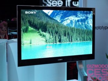
Sony OLED TV prototypeSony OLED TV prototype

The report also details the collaboration between Panasonic and Sony. The two companies have quite different technologies - Panasonic with its P-OLED and printing processes and Sony with small-molecules and VTE. It is claimed that Sony will mostly supply capital for Panasonic, and not technology. Sony's own OLED technology will be used though by Japan Display to make small sized panels.

Read the full story Posted: Sep 12,2012

Introduction to LECs, a cheaper and flexible alternative to OLEDs

One of the promises of OLED lighting is that flexible panels can be produced on the cheap using roll-to-roll processes. There is a lot of work towards this goal, but it hasn't been achieved yet. Now researchers from Sweden and Denmark have managed to produce light-emitting electrochemical cells (LEC) using an all-solution-based R2R fabrication process, in ambient conditions. They say that this process can be used to create large area panels too.

Polymer LEC panels are similar to PLEDs in structure, but in LECs the emitter polymer is blended with an electrolyte (e.g. LiCF3SO3 dissolved in PEO). LECs, which require only three layers, were first reported 15 years ago, but they suffered from very low lifetime and efficiency. But LECs are very easy to produce and so with steady improvements (mostly from choice of electrodes) LECs are now ready to enter the lighting market.

Read the full story Posted: Sep 09,2012 - 2 comments

Tailoring wettability results in better inkjet-printed electronics structures

Researchers from the Fontys University in The Netherlands have demonstrated that patterned plasma treatment of substrates gives them better control over inkjet printed structures (which results in higher quality printing).

The researches have used tailored wettability using InnoPhysics uPlasmaPrint technology that can locally change surfaces from hydrophilic to hydrophobic and vice-versa, creating patterns that make droplets spread in only one direction while restraining them in the other direction. Printed lines created in this way have both a very high homogeneity and a well-controlled width (without this technology the inkjet spreads in all directions which creates broader lines). In the research they used PixDro's LP-50 R&D inkjet printing platform.

Read the full story Posted: Sep 07,2012

Does the Galaxy Note 2 use Ignis' AdMo-p technology?

Yesterday I posted about the Galaxy Note 2 subpixl scheme, with the 5.5" 1280x720 HD Super AMOLED display featuring 267 ppi (with three subpixels per pixel). Our readers pointed out that the new scheme used in the Note 2 looks very much like Ingis Innovations' patented HR pixel structure (as part of their AdMo-p technology). This may explain how Samsung managed to get good enough lifetime at such a high PPI without PenTile.

Just as a reminder, here's how the Note 2 pixels are arranged. It's not exaclty the same as in the HR structure as the red and green sub-pixels have the same size. In any case:

Read the full story Posted: Sep 06,2012 - 1 comment

AUO reached 50% yield in AMOLED fab, ready to start mass production

According to Digitimes, AUO managed to achieve 50% yield in its AMOLED fab, and is set to start mass production - on track with AUO's plans to start AMOLED mass production in Q3 2012 (but a delay from the original plan). AUO will make 4.3" qHD panels (257 ppi). AUO is co-developing in-cell touch AMOLED panels together with some handset makers (some suggest the main customer for AUO's OLEDs is HTC).

AUO's current capacity is about 7,000 monthly substrates in their Gen-3.5 fab. Later on the company plans to bring their Gen-4.5 fab in Singapore (at AFPD) online with a monthly capacity of 15,000 substrates.


Read the full story Posted: Sep 06,2012

Samsung sues LG Display over OLED technology leak

Samsung Display filed a lawsuit against LG Display over OLED technology tech leak. Samsung Display claims that LG Display stole 18 confidential technologies relating to OLED displays, demanding a billion won (almost $900,000) for each technology. Samsung also said that LG Display gave some information to a third party.

In July we reported that 11 former and current Samsung employees were charged of giving LG Display confidential OLED technology, and this is Samsung's reaction in court. Actually, it seems strange that Samsung is only seeking about $17 million dollar in damages - this seems to be a very small amount when you consider that the OLED display market is now estimated to be about $6 billion, and is set to grow to about $44 billion by 2019.

Read the full story Posted: Sep 06,2012