Technical / Research - Page 48

Samsung to launch Full-HD AMOLED mobile displays at 400 PPI next year?

Korean site MK news reports that Samsung have plans to produce Full-HD AMOLED panels in the first half of 2012. These panels will feature a pixel density of 400 ppi or even more. Just to compare, the highest PPI AMOLED ever made is the one used in Samsung's own Galaxy Nexus (316 ppi: 4.65", 1280x720, with PenTile technology). The S3 has 306 ppi( 4.8" 1280x720, PenTile) and the Note II has only 267 ppi, 5.5" 1280x720 - but without PenTile.

Back in July it was reported that Samsung managed to reach 350 ppi using FMM (Fine Metal Mask) technology. Perhaps they are getting close to commercialize this specific technology (and also increase the resolution even further to 400 ppi).

Read the full story Posted: Oct 23,2012 - 2 comments

Fraunhofer and POG co-developed micrometer-coated OLED structures on glass

Fraunhofer's COMEDD and POG Präzisionsoptik Gera have co-developed OLED structures coated in the range of micrometers at opaque or transparent glass substrates. This technology can be used in complex optical and opto-electronical systems in a range of applications (medical, laser, aerospace, telescopes, microscopes and even sports optics). Basically these are transparent optical devices with self-emitting figures, points or lines;

The best technology used today to achieve the same effect uses prisms. The advantage the new design is that the active luminous area is integrated directly into the glass substrate which results in a better field of view, and the whole system is much more simple - and hopefully will result in cheaper designs.

Read the full story Posted: Oct 15,2012

Ignis demonstrates their MaxLife external compensation technology

Back in June 2012 I reported from SID on Ignis' Max Life technology. Max Life provides external compensation - that deals with OLED burn-in. The idea is to keep track of how much each pixel was used, and so it's possible to calculate the brightness loss in that particular pixel, and then drive this particular pixel correctly - to compensate. Ignis now released a nice video showing a 20" AMOLED panel (their own a-Si prototypes made by RiTDisplay) with a burn-in logo. When Max Life is turned on, the logo disappears:

Ignis explains that while Max Life theoretically makes the "eventual" lifetime (until the display burns out completely) worse, in practice it helps to make the device usable longer. Ignis says that the main problem is non-uniformity in brightness and not actual brightness.

Read the full story Posted: Oct 11,2012 - 1 comment

Cynora unveiled a new flexible OLED prototype aimed for smart packaging

German startup Cynora unveiled a new mostly-solution-based flexible OLED prototype - aimed for smart packaging applications. Cynora developed the low-cost emitters (based on copper precursors) and developed the prototype in collaboration with InnovationLab (in a project titled cyFlex).

Cynora are now working towards the integration of the wiring into the thin film layers of the OLED. Cynora are using solution processing (coating and printing).

Read the full story Posted: Oct 09,2012

AIST developed an new method to measure OLED molecule behavior while the device is working

Researchers from the Japanese National Institute of Advanced Industrial Science and Technology (AIST) developed a new method to selectively measure the behavior of specific molecules at the interfaces of organic layers in a multilayered OLED device - while the device is emitting light, and without harming the device. This can be used to study the deterioration of materials and interface in the OLED and enable improving the device's lifetime easier.

The researchers used advanced laser spectroscopic technique to measure the molecular vibrational spectrum at each layer interface. More specifically, they have used sum frequency generation (SFG) spectroscopy. AIST developed a two-color SFG spectroscopy that uses wavelength-tunable lasers.


Read the full story Posted: Oct 09,2012

Futaba shows a new flexible PMOLED prototype at CEATEC 2012

Futaba unveiled a new 3.5" (256x64) full-color flexible PMOLED prototype. The new prototype is thin (0.22 mm thick - thinner than Futaba's current 0.29 mm thin panels) and features 100 cd/m2 brightness.

This seems to be quite similar to the old flexible OLED panel shown at CEATEC 2010 by TDK Micro (now owned by Futaba), but it's quite a bit thinner (back in 2010 the panel was 3 mm thick). The old panel was made on a resin substrate and used a white emitter with color filters. We do not know the technology used in the new panel.

Read the full story Posted: Oct 08,2012

UDC contracted Duksan Hi-Metal to produce OLED host materials in Korea

Universal Display announced that it has contracted Duksan Hi-Metal to produce OLED host materials in Korea. The two companies have entered into a "master services agreement". The first initiative under the new agreement is to provide manufacturing services for "one of Universal Display’s host products for certain Korean customers". This is most likely a green host material for Samsung Display.

Samsung is already using UDC's green emitter and host materials in some OLED displays (the PSP Vita and the Motorola Droid RAZR smartphones) and is set to start using it in more products in the future with an aim to reduce the power consumption of its OLED displays. Having a green host manufacturer in Korea will enable UDC to lower the price of its material, and it's always good to have a 2nd supplier (all of UDC materials are currently produced by PPG Industries).

Read the full story Posted: Sep 27,2012

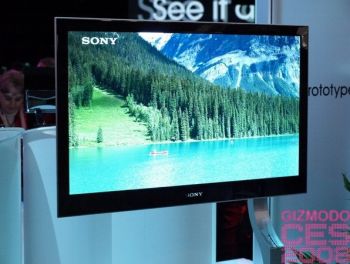
Sony and Panasonic to offer OLED TVs by March 2014

According to Sony's home-entertainment product chief, Masashi Imamura, the OLED collaboration with Panasonic is "running smoothly". The two companies may offer OLED TV products after March 2014.

Sony OLED TV prototypeSony OLED TV prototype

Sony and Panasonic announced their OLED technology partnership in June 2012 - saying that the two companies will jointly develop printing based technologies for OLED TV mass production. According to the original plans, the technology will be "established during 2013", but obviously setting up a mass production facility will also take time.

Read the full story Posted: Sep 27,2012

AUO is looking into an OLED printing process

Digitimes reports that AUO has started to develop a printing process to make OLED panels, with hopes that this new process will lower the production cost and increase the material utilization. AUO is suffering from low (50%) yields in its current production process - which uses vapor deposition. The report suggests that AUO is also developing Oxide-TFT backplanes for OLEDs - but this isn't news - AUO unveiled an Oxide-TFT based 32" OLED TV prototype back in November 2011.

AUO 32-inch AMOLED prototype

Actually all OLED makers are looking into more efficient production processes based on printing so this is hardly a surprise. It's likely that it will take some years before we'll start seeing printed OLED panels on the market though.

Read the full story Posted: Sep 27,2012