FMM - Page 2

Reports from Korea suggest that Samsung Display is interested in acquiring SEL's mask-less OLED production technology

According to reports from Korea, Samsung Display is interested in acquiring OLED IP and patents from Semiconductor Energy Laboratory (SEL). These patents detail an OLED production process that does not require the use of fine metal mask (FMM) evaporation.
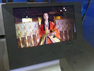
SEL 8.3-inch 8K OLED prototype (Dec 2018)

The use of FMM to deposit and pattern OLED displays is seen as a major setback towards higher density OLED displays, and it also limits the aperture ratio. It is no wonder that Samsung is interested in such technology, as other display makers have developed similar technologies that offer massive performance boost over the standard FMM process.
Read the full story Posted: Jul 26,2023

Visionox new ViP OLED technology uses photolithography-based patterning to increase display performance

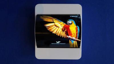
Visionox is introducing a new OLED production technology, called Visionox Intelligent Pixelization (or ViP for short) that enables higher-density display production, at over 1,700 PPI.

The idea behind ViP is to replace the fine metal mask (FMM) method with photolithography-based pixel patterning. The process offers several advantages, mainly the increase of aperture ratio to almost 70% (Visionox says the currently reach 69%). FMM methods usually achieve up to 30%, which means that brightness, efficiency and lifetime can all be increased.

Read the full story Posted: May 10,2023 - 2 comments

HKC to start making AMOLED displays in collaboration with JDI using its eLEAP production technology

In 2022, Japan Display (JDI) announced that it has developed a "historic breakthrough in display technology" - a new OLED deposition process which they refer to as eLEAP, that is said to be cost effective and can be used to create freeform OLEDs that are brighter, more efficient, and longer lasting compared to OLEDs produced using mask evaporation (FMM).

JDI eLEAP aperture ratio image

We now hear that China-based LCD maker HKC Corp has signed an agreement with JDI to adopt its technology for mass production of AMOLED displays. Under the agreement HKC will invest billions to build AMOLED factories in China, while JDI will provide the manufacturing expertise and technologies, including eLEAP. The plan is to begin mass production in 2025, with the first applications to be in automotive displays and wearable devices.

Read the full story Posted: Apr 12,2023

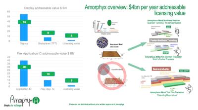
Amorphyx Q&A about champion performance in IGZO TFT for OLED Smartphone applications

This is a sponsored post by Amorphyx, where display industry consultant Ian Hendy has interviewed Amorphyx's CEO John Brewer

Q: Can you start by telling us a little about what Amorphyx does, John?

Amorphyx has several fundamentally new technology platforms that provide for TFT performance improvements in three areas: (1) Switching speeds, with options to move to the Tera-Hz range ultimately, (2) Power, where the IGZO AMeTFT can achieve even lower power performance than today’s LTPO OLED Pro Motion displays and better refresh range, and (3) Small transistor size.

Our technology platforms are lower cost than the alternatives, and move from amorphous and crystalline semiconductor approaches, to devices based on different effects that do not have a semiconductor at all, yet can still drive a display, drive current, deliver grey scale and switch very fast. Or they can operate a flex IC at higher clock speeds than known today.

For now, our main commercial focus is on IGZO AMeTFT which is fundamentally a potential replacement transistor for LTPS or LTPO used in modern OLED phones and has the capability to replace more highly compensated LTPO circuits in modern Smartphone displays due to enhanced stability.

Read the full story Posted: Jan 08,2023

DNP invests $140 million to increase its OLED FMM production capacity

Japan-based Dai Nippon Printing (DNP), the world's leading OLED FMM mask producer, is investing about 20 billion Yen (about $140 USD million) to expand the production capacity at its Kurosaki plant situated in Kitakyushu City.

DNP Kurosaki plant at Kitakyushu City photo

DNP says that the new FMM line is expected to begin production in the first half of 2024, and will produce large-area FMM masks, suitable for the 8-Gen lines now being commissioned by the OLED industry to enhance production for IT displays. This new capacity will more than double DNP's FMM production capacity.

 
Read the full story Posted: Nov 10,2022

A report suggests that Samsung Display is interested in JDI's eLEAP OLED deposition technology

A few months ago, Japan Display (JDI) announced that it has developed a "historic breakthrough in display technology" - a new OLED deposition process which they refer to as eLEAP, that is said to be cost effective and can be used to create freeform OLEDs that are brighter, more efficient, and longer lasting compared to OLEDs produced using mask evaporation (FMM).

JDI eLEAP aperture ratio image

According to a new report from Korea, Samsung Display is interested in JDI's new technique. Interestingly the report shows conflicting views within SDC - some are interested in adopting this new technology, especially at SDC's upcoming 8-Gen IT OLED production line, while others are more interested in preventing SDC's competitors (JDI, or others?) from using it, perhaps by pressuring OLED equipment makers to not offer needed equipment to JDI.


Read the full story Posted: Sep 21,2022 - 1 comment

APS Holdings to build an OLED microdisplay R&D production line, aims to reach 3000 PPI via FMM by 2023

In 2021 The Korean government launched a new project that aims to develop technologies for the production of OLED microdisplays for AR applications. The project is led by AP Systems (APS Holdings), and aims to produce a direct emission OLED microdisplay with a resolution of 4,000 PPI by 2024.

According to reports from Korea, APS Materials has managed to develop a 1,000 PPI FMM mask, and is now building a new R&D line that will be used to produce direct emission OLED microdisplays using FMM technology. The new APS production line will include OLED deposition and encapsulation.

Read the full story Posted: Jun 17,2022

Japan Display announces a breakthrough lithographic-based OLED production method

Japan Display (JDI) announced that it has developed a new OLED deposition technology, which they refer to as eLEAP, that is cost effective and can be used to create OLEDs that are brighter, more efficient, and longer lasting compared to OLEDs produced using mask evaporation (FMM). eLEAP also enables OLED freeform deposition. JDI regards its new technology as a " historic breakthrough in display technology".

JDI eLEAP aperture ratio image

eLEAP is based on a lithographic method, and does not require any masks. The main advantage seems to be that OLED displays produced by eLEAP technology can achieve an aperture ratio of 60%, compared with FMM OLEDs which achieve a ratio of about 28%. This means that the OLED displays can be driven at lower currents - which extends the lifetime, improves the efficiency and also enables higher-peak brightness when needed.

Read the full story Posted: May 15,2022

Researchers use a 3D OLED pixel configuration to increase efficiency by up to 30%

Researchers from National Taiwan University, led by Prof. Chung-Chih Wu, have developed a 3D pixel configuration for OLED devices, which can improve the light extraction. The new design can improve the external quantum efficiency of a top-emitting OLED device by up to 30%.

Reflective 3D OLED pixel configuration (NTU)

The new design uses a 3D reflective pixel structure filled with a patterned high-index material. The researchers created several pixels with difference sizes, and found that the smaller the pixel, the higher the efficiency boost.

Read the full story Posted: Feb 01,2022

OLEDON developed a curved plane-source FMM technology that can be used to produce direct-emission 10,000 PPI OLED microdisplays

OLEDON says that it has developed a new curved plane-source evaporation shadow mask process that can be used for OLED microdisplay fabrication, with a potential density of 10,000 PPI (minimum shadow distance of 0.18um). Using this technology it will be possible to create direct-emission microdisplays.

In the video above, you can see the lecture OLEDON's CEO gave last month at iMID 2021, that explains the new technology.

Read the full story Posted: Dec 24,2021