Technical / Research - Page 43

eMagin introduce the new OLED-XLS series, the world's brightest full-color OLED microdisplays

eMagin unveiled the world's brightest full-color OLED microdisplays, the color OLED-XLS series. Those displays offer 1000 nits of luminance, that is four times brighter than "current industry standard".
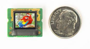
XGA096 OLED-XL

eMagin are currently offering OLED-XLS displays in sample quantities over their entire product line (VGA, SVGA, XGA, SXGA and WUXGA). They will continue to produce the "older" OLED-XL displays.

Read the full story Posted: Jun 15,2013

nVerPix updates on their CN-VOLET backplane technology and business

Back in 2011 the University of Florida announced a new organic-TFT backplane technology called CN-VOLET, which is especially suited for OLED panels. Earlier in 2010, the University spun-off a company called nVerPix to commercialize this technology, with funding from Nanoholdings. Now nVerPix sent us some information and updates regarding their technology and business as they are seeking to raise funds (Round A).

CN-VFET is a new carbon nanotube based transistor technology that can conduct electricity about a 1000 times faster than current silicon-based TFTs. The basic transistor design is called CN-VFET (which can be used for logic and memory applications). When they combine the CN-VFET with the OLED stack they call it a CN-VOLET (CN Vertical OLET).

Read the full story Posted: Jun 10,2013

iOLED: NHK and Nippon developed a new OLED structure that offers better oxygen and moisture resistance

Japan Broadcasting Corp (NHK) and Nippon Shokubai developed a new OLED structure (called inverted OLED, or iOLED) that drastically improves oxygen and moisture resistances. The two companies demonstrated a prototype 5" QVGA (320x240, 80 PPI) red monochrome panel that uses the new structure.

The basic iOLED idea is to invert the structure between the electrodes of a bottom-emission OLED. So in an iOLED, on top of a transparent negative electrode (ITO), you place the EIL, ETL, emitter layer, HTL and finally the positive electrodes. According to the two companies, this structure makes the OLED more resistant. The brightness (or light emitting area) of a normal OLED will decrease by half within 100 days if it is exposed to air (due to the oxidation of the negative electrode). An iOLED will will hardly deteriorate in these conditions.


Read the full story Posted: Jun 05,2013 - 1 comment

The US DoE awards $3.3 million to PPG and OLEDWorks in two new OLED lighting projects

The US Department of Energy (DoE) awarded $10 million to five solid state lighting projects. Two of these projects are OLED lighting ones. The first project, worth $2.3 million, was awarded to PPG Industries. PPG will develop a cost-effective manufacturing process to help commercialize an integrated substrate (which includes the glass foundation and the other necessary layers).

PPG's project will use standard grade glass which should lower the cost (while maintaining the performance) compared to the high-end glass used in OLED today. This is PPG's second grant from the DOE. In January 2010, the DOE awarded $1.6 million to develop "Low-Cost Integrated Substrate for OLED Lighting". This program is now finished and PPG has been recognized by the DOE for significant achievements in advancing OLED lighting technology.

Read the full story Posted: Jun 05,2013

LG Chem's 60 lm/W OLED lighting panels now feature high CRI (over 90)

LG Chem announced that since April 2013, all its OLED panels have a CRI of over 90. CRI determines a light source ability to reproduce colors on which the light shines, and a high CRI means a "high light source quality".

LG Chem says that generally, CRI and efficiency are trade-off factors, but LG Chem managed to maintain high panel efficiency (60 lm/W), color temperatures between 3000K and 4000K and lifetime at 20,000 hours.

Read the full story Posted: Jun 02,2013

Fraunhofer COMEDD developed color-tunable OLED lighting panels

Fraunhofer's COMEDD developed new color tunable OLED lighting panels. These new panels will be presented at the LOPE-C 2013 exhibition (June 11) for the first time. To develop these new panels, the Fraunhofer used vertical stacking of OLED emitters which can be controlled separately.

They say that by using different process technology, COMEDD was able to achieve the right stack architecture including the optimized thickness of the individual OLEDs for an appropriate efficacy.

Read the full story Posted: Jun 02,2013

CPI posts some updates on their OLED developments

The UK's Centre for Process Innovation (CPI) posted some updates on their OLED program. They have recently produced defect free OLED lighting samples. They managed to produce panels that has large (over 250 cm2) emissive areas (they are producing these panels on 8" substrates and so could exceed 160x160 mm panels).

CPI 154x154 OLED lighting sample photo

The CPI developed two kinds of panels - the first uses small molecule materials and the second uses full solution-processable PLED materials. They have also produced samples that use a hybrid structure with a PEDOT layer (deposited using a slot die process) with an evaporative emissive layer (that has better efficiency and performance compared to the PLEDs). The 154x154 mm example shown above is the hybrid structure.

Read the full story Posted: Jun 02,2013

NHK developed a 8" flexible OLED panel prototype

NHK's Science & Technology Research Laboratories (STRL) unveiled a new 8" flexible OLED prototype panel. The panel features a resolution of 640x480 (100 ppi) and is based on an amorphous InGaZnO (a-IGZO) TFT backplane.

STRL says that the red emitter material is a new phosphorescent material that is made from a benzoquinoline derivative host doped with a platinum based complex. The encapsulation is made from a polymer material.


Read the full story Posted: Jun 02,2013

The European Smartonics project will use Aixtron's OVPD system

Aixtron announced that the European Smartonics project (which aims to develop smart machines, tools and processes for the precision synthesis of materials for organic electronics) will use the company's OVPD evaporation process and roll-to-roll printing machines. Aixtron is one of the project's partners and they will develop a small R&D OVPD cluster system that will use the company's latest 200 mm R&D platform, which is optimized and qualified for manufacturing of organic photovoltaic devices.

PRODOS R&D system

OVPD (Organic Vapor Phase Deposition) organic material deposition technology was developed by Universal Display. Aixtron holds an exclusive license to produce OVPD manufacturing equipment.

Read the full story Posted: May 29,2013 - 1 comment

Toshiba, Panasonic and the FDC developed new flexible OLED panels

Several companies announced new flexible OLED panels at SID 2013. None of the panels were demonstrated (except for Toshiba which showed the OLED but it was not powered). First up is Toshiba, which showed a 10.2" 1920x1200 (223 PPI) panel. Toshiba's OLED has an Oxide TFT backplane and uses the WRGB (white OLED with color filters) architecture.

Toshiba flexible OLED prototypeToshiba flexible OLED prototype

Panasonic developed a 4" flexible OLED with 224x224 resolution (only 80 PPI, direct emission). Panasonic used PEN as a substrate and the panel can be bent up to a curvature radius of 10 mm. This is also an Oxide-TFT panel. To produce it, Panasonic attached the PEN sheet to a glass substrate, deposited the OLED materials and then de-laminated the glass.

Read the full story Posted: May 26,2013