Technical / Research - Page 30

The EU launches a new project to commercialize TADF OLED emitters

The European Commission, under its Horizon 2020 programme, launched a new project called Phebe that aims to develop and commercialize TADF OLED emitters. This three-year project's consortium includes Novaled, Astron-FIAMM, TU Dresden, Kaunas University of Technology, Durham University and other companies and universities.

TU Dresden is focusing on material design using theoretical quantum chemical approaches, and KTU is elaborating synthetic schemes for exciplex emitters and intramolecular charge transfer materials and synthesizing the most promising compounds. Durham will perform photophysical characterisation of the new materials from Kaunus and will also be in charge of elucidating the mechanisms of TADF to feed into the theoretical work of TU Dresden. Novaled will provide best-fit transport and doping material sets, technology and expert know-how on stack architecture.

Read the full story Posted: Mar 19,2015

The US DoE awards two new SBIR phase-two OLED projects

The US Department of Energy (DoE) awarded two small-business SBIR Phase-2 projects targeting advances in solid-state lighting technology, and both projects deal with OLED lighting technologies.

The first project, led by Pixelligent Technologies is titled "Advanced Light Extraction Material for OLED Lighting". Pixelligent, in collaboration with OLEDWorks, will demonstrate a new internal light extraction structure for OLED lighting panels, that is fully compatible with current manufacturing processes and operating conditions. The ILE structure is cost-effective and offers a high high refractive index.

Read the full story Posted: Mar 09,2015

Finely patterned OLEDs are brighter and more efficient, may enable organic lasers

Researchers from Japan (Chihaya Adachi of Kyushu University) and California have shown that OLED devices made with finely patterned structures are brighter and more efficient compared to regular OLEDs. The key finding in their research is that when the charge transport and recombination are confined to small nanoscale areas, the electroluminescent efficiency is increased because roll-off is suppressed.

The researchers say that such a structure (which are made using electron-beam lithography) may finally enable OLED devices to be bright enough and efficient enough to be used as laser sources. The researchers fabricated a small OLED device that supports charge density injection of 2.8 kA/cm2 while maintaining 100 times higher luminescent efficiency than previously observed.


Read the full story Posted: Mar 08,2015

VTT researchers develop low-cost polymer OLED lighting deposition technology

Finland's VTT Technical Research Centre developed a new technique to deposit patterned OLED lighting elements on flexible plastic films. This could enable a low-cost process technology to make flexible light emitting structured films - which they see used mostly in advertisement campaigns.

VTT printed polymer OLEDs photo

The new room-temperature deposition technology uses standard traditional gravure and screen printing - which means it may be possible to use in regular printing houses. The process makes OLED lighting stripes which are 0.2 mm thick and uses polymer based OLED emitters.

Read the full story Posted: Mar 08,2015

DuPont updates us on their OLED advances, sees printed OLED TVs soon

DuPont has been working on OLED materials and processes for a long time, but it's been a while since we heard any update. David Flattery, DuPont's OLED unit Director of Operations was kind enough to update us on the company's materials and OLED technologies.

Q: Dave - thanks for this interview. We know that DuPont is focusing on soluble OLED materials and processes. When do you see the OLED display industry starting to adopt such materials?

DuPont is focused on developing OLED materials for evaporation and soluble technologies, as well as working with our partners on our proprietary printing process.

Many in the industry believe that 2017 will be the year of mass production for printed OLED televisions, and while we cannot disclose the manufacturing plans for our partners, we have already seen one large manufacturer announce that they will pilot solution- processed OLED displays up to gen-8 in 2015.

Read the full story Posted: Feb 04,2015 - 2 comments

Kateeva and Sumitomo to pair PLED materials to Kateeva's ink-jet system

Kateeva and Sumiomo Chemical announced a non-exclusive key partnership to pair Sumitomo's PLED materials to Kateeva's YieldJet OLED ink-jet printing platform. The two companies hope this collaboration will lead to adoption of P-OLED inkjet printing by OLED TV makers.

Kateeva and Sumitomo will cooperate to co-develop high-quality reference data for customers, which will be optmized to Kateeva's platform and Sumitomo's inks.

Read the full story Posted: Jan 15,2015

Researchers develop an all-organic pulse oximeter sensor

Researchers from UC Berkeley developed a pulse oximeter sensor that is made entirely from organic optoelectronics. The flexible oximeter can measure arterial oxygen saturation and heart rate, and performs as well as silicon-based pulse oximeters.

Organic-electronics pulse oximeter photo

The sensor is made from red and green flexible OLED lighting devices and an organic photodiode (OPD). Unlike regular devices, this new organic sensor device is thin, flexible and (theoretically) cheap.

Read the full story Posted: Dec 22,2014

Royole shows a 0.01 mm thick flexible AMOLED prototype

Royole, a startup established in the US in 2012, unveils their first prototype, a 0.01 mm thick (thin?) flexible AMOLED prototype (which they say is the thinnest ever). Here's a video showing the display in action:

The display is bendable, and has a bending radius of 1 mm. Samsung's recent flexible AMOLED prototypes has a radius of 5 mm - but these prototypes are closer to production units (the flexible OLED in the Galaxy Note Edge has a radius of 7 mm). Samsung's aim is to achieve a radius of 1 mm in production within two years.

Read the full story Posted: Dec 17,2014

Seiko Epson developed a 360 PPI OLED ink-jet printer head, now developing a 600 PPI one

According to OLEDNet, Seiko Epson developed a new OLED ink-jet printer head that can achieve a resolution of 360 PPI. This high-density print head uses two 180 PPI nozzles in 2 offset rows. The company managed to print prototype bottom-emitting and top-emitting OLED devices using this print head.

OLEDNet says that Seiko Epson is now aiming to develop a 600 PPI ink-jet printer head, by using two rows of 400 PPI nozzles.

Read the full story Posted: Dec 16,2014

Korea researchers develop strong, more precise shadow masks for OLED manufacturing

Researchers from the Korean Inha University developed a new method to produce shadow masks that could lead to masks that have higher densities and are also more robust - leading to higher yields in OLED production. The team are going to transfer the technology to a company that will commercialize it.

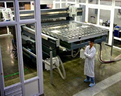
Samsung AMOLED productionSamsung AMOLED production

The researchers used an electrochemical processing technique to manufacture the new masks. This enables masks that are stronger (and thus fail less often) and still reach pixel densities of up to 500 PPI.

Read the full story Posted: Dec 11,2014