ALD

Ergis updates on the status of its noDiffusion OLED encapsulation film

This is a sponsored post by Ergis Group

In 2020, Poland-based Ergis Group launched the noDiffusion film platform, a high-barrier film that offers high level of optical transmittance and low level of light scattering, and the ability to contain transparent conductive electrodes. The new technologies adopted in the production of the barrier films offer a combination of high performance and competitive pricing.
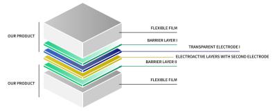
Ergis noDiffusion structure

Ergis has been busy since 2020, scaling up its production capabilities, and progressing towards production in a roll-to-roll configuration (rather than the batch system it used before). Ergis is using two different technologies - ALD and sputtering to deposit the barrier and the conductive electrodes.

Read the full story Posted: Jun 13,2023

Merck launches new highly-effective ALD OLED encapsulation materials

Merck introduces new OLED encapsulation materials that the company says offer superior flexibility, higher reliability, and longer lifetime for flexible devices compared to existing solutions. 

Merck says that its new low-temperature ALD silicon materials offer highly improved barrier characteristics - 100 times more effective than current solutions. And they can be deposited in thin layers - 20 times thinner than existing solutions. Merck introduced low-temperature ALD silicon materials in 2022 for automotive OLED, and the company expects that the new materials will be used for the encapsulation of flexible IT OLED displays (laptops, tablets and monitors).

Read the full story Posted: Jun 02,2023

Holst Center researchers use sALD to create IGZO OLED display backplanes on PEN foils

Researchers from the Holst Center has applied spatial atomic layer deposition (sALD) to create both the semiconductor and dielectric layer in a thin-film transistor (TFT) Oxide-TFT (IGZO) display backplane - for the first time ever.

Holst sALD QVGA OLED prototype photo

The researchers created a 200 PPI QVGA OLED display prototype on a thin PEN foil. This shows how TFTs can be produced in a low temperature process (below 200 degrees Celsius) using sALD on a cheap transparent plastic foil. The TFTs achieved a mobility of 8 cm2/V2 with channel lengths down to 1 um.

Read the full story Posted: Nov 18,2019

SALDtech announces its 2nd investment round, to develop flexible OLED deposition tools

SALDtech logoThe Netherlands based SALDtech, established in 2018 as a spinoff from the TNO institute, announced that it closed its 2nd financing round led by Innovation Industries and BOM, Brabant Development agency.

SALDtech developed deposition tools based on the Holst Centre's Spatial Atomic Layer Deposition that can be used to produce large area ultra-thin layers with world class performance. SALDtech says it will used the investment to develop and build flexible OLED production equipment.

Read the full story Posted: May 27,2019

KAIST researchers develop a washable wearable solar-powered OLED device

Researchers from the Korea Advanced Institute of Science and Technology (KAIST) developed a self-powered wearable and washable OLED display device. The whole device is fabricated on textiles and the efficient OLED devices are driven by polymer solar modules.

Washable and wearable PSC and OLED device (KAIST)

Both the OLED device and the polymer solar panels are sensitive to moisture and oxygen, and regular OLED encapsulation will not protect such a device when washed. The researches designed a new washable encapsulation barrier using both ALD and spin coating. The device is flexible (curvature radius of 3 mm) and survived 20 washing cycles of 10 minutes each with little change in performance.

Read the full story Posted: Mar 28,2019

Graphene-based barrier demonstrated as a possible solution for flexible OLED encapsulation

Graphene is the world's most impermeable material, and as the material is also transparent, flexible and ultra-thin it makes sense to adopt graphene as an encapsulation layer for next-gen OLED displays. A UK project led by Cambridge University researchers have set out in 2015 to develop such a solution, and the researchers now report that they have demonstrated a viable graphene solution comparable to existing commercial OLED encapsulation technologies.

Graphene encapsulation research, CPI 2017

In its pure form, graphene is permeable to all gases, but real life materials are never entirely pure and defects and holes harm the material's permeability. The new research used ALD and CVD to create large-area high-quality single-layer graphene sheets which were stacked to create a multi-layer coating. The researchers say that a ~10 nm barrier layer that includes 3-4 layers of graphene (with AlOx in between) is an effective solution for OLED displays. The 10 nm layer maintains a high optical transparency (>90 %) and high flexibility.

Read the full story Posted: Oct 27,2017

UBI Research sees PECVD as the in-organic TFE equipment of choice for flexible OLED production

UBI Research says that as OLED makers are diverting all efforts into flexible OLED production, thin film encapsulation (TFE) is gaining in popularity. Between 2017 and 2021, TFE will be applied to about 70% of all OLED panels in production. The OLED encapsulation equipment market will generate $11 billion in sales.

PECVD oled encapsulation market share (UBI, 2017-2021)

TFE encapsulation started out as a complex technology that required 11 layers and was slow and expensive. Recent advances allowed OLED makers to reduce the number of layers to just 3 and increase productivity and yields and so lower the production costs. Some film OLED makers opted for hybrid encapsulation (which uses a barrier film) but TFE seems to have become the technology of choice.

Read the full story Posted: Jul 29,2017

Encapsulix to supply ALD-TFE equipment to a leading Asian AMOLED producer

ALD equipment maker Encapsulix announced that a leading Asian AMOLED manufacturer has chosen its ALD-TFE deposition systems, to be used as flexible AMOLED encapsulation. The first tool is already under construction and will start operating in the spring of 2017.

Encapsulix says that the order was awarded following an extensive evaluation of available ALD platforms, and this confirms the technological superiority and leading cost-of-ownership of the company's ALD-TFE equipment.

Read the full story Posted: Jan 23,2017

The Holst Center developed a Spatial-ALD TFT deposition process

Researchers from the Holst Centre developed a new process to deposit semiconductor layers with better performance and high throughput than PVD-based process. the new process is based on scalable, atmospheric-pressure process spatial-ALD.

Display transistors deposited by sALD image

The Holst Centre used sALD to deposit IGZO backplanes that achieved charge carrier mobilities of 30 to 45 cm2/Vs. The researchers say that similar backplanes deposited with PVD (supttering) achieve about 10 cm2/Vs. The sALD layers also exhibited low off current, switch-on voltages around 0 V and excellent bias stress stability.

Read the full story Posted: Nov 24,2016

Researchers develop a cheap and efficient MgO-based OLED encapsulation layer

Researchers from South China University of Technology (SCUT) demonstrated a new MgO-based OLED encapsulation layer. The researchers say that MgO provides an efficient barrier at a low cost, and can be deposited in low temperatures.

MgO OLED encapsulation tests (SCUT 2016)

The researchers say that this is the first time that MgO is used for OLED encapsulation, but this material has a number of advantages - a low refractive index, a wide bandgap, high dielectric constant, high chemical stability and the lack of UV irradiation treatment requirements.

Read the full story Posted: Nov 11,2016