OLED ink jet printing: introduction and market status - Page 19
Kateeva expands their Korean operation
Kateeva announced that the company is expanding its Korea operation, by absorbing the assets of Seoul-based OLED Plus - an OLED equipment design, sales, service and support company headed by OLED industry veteran, KB (Kyung Bin) Bae, who will become the general manager of Kateeva Korea, a wholly owned subsidiary of Kateeva.

Two months ago Kateeva unveiled their YIELDJet OLED ink-jet printing system. The company now says that interest in this technology is high - especially in Korea, and commercial shipments are "imminent".
Merck and LG Display to co-develop OLED printing materials?
Reports from Korea suggest that LG Display and Merck are in talks to co-develop OLED ink jet printing materials. Merck is already supplying evaporable OLED materials to LG Display for their OLED TVs, and now they want to also supply soluble materials for LGD.

Merck is focused on OLED printing technologies over evaporation technologies as the technological advantages will enable cheaper large area panels. According to a Merck presentation released earlier this year, it seems that Merck wants to become an OLED solution provider, not just a material supplier as this will maximize the value for both Merck and its customers. The company currently has around 80 OLED R&D experts and around 1,400 related patents.
Kateeva finally unveil their YIELDjet OLED TV inkjet printing system
Kateeva is a US based startup that was established in 2009 to develop OLED ink-jet deposition technology originally developed at MIT. The company has been been in stealth-mode for years, and now finally they have unveiled their technology and system, branded YIELDJet.

So YIELDJET is an inkjet printing system that can be used to produce OLEDs in high volume. Kateeva claims that their system, the first one engineered from the ground up for OLED mass production, will dramatically improve yields and drive production costs lower. Kateeva says that this was achieved by three major technical breakthroughs: is features a production-worthy pure nitrogen process chamber, which doubles the lifetime in certain applications, it reduces particles by as much as 10X thanks to a specialized mechanical design and it offers exceptional film coating uniformity with a process window that’s 5X wider than standard technologies.
Fraunhofer IAP and MBraun develop an OLED lighting and OPV printing system
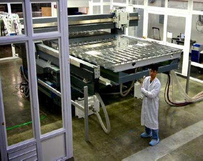
Researchers from the Fraunhofer IAP insitute, together with MBraun, developed a new production facility that can be used to print OLED panels and OPV cells. They say that the new system can be used to produce large sample panels. The Fraunhofer showed the "bus stop of the future" that includes both large OPVs and OLED displays:

The Fraunhofer released very little technical details. I think this process actually produces very large OLED (or OPV) pixels , so you can think of these as OLED lighting panels and not really displays. The researchers said that the system includes a robot that controls different printers - and this all is like a "huge" ink-jet printer.
BOE plans a 8-Gen Oxide-TFT WRGB AMOLED line in Hefei
China's BOE Display is building a 5.5-Gen LTPS fab in Ordos by the end of 2013. This fab will first produce LTPS LCDs, but BOE wants to switch it to AMOLED production. According to OLEDNet, during the FPD International 2013, BOE's Dawei Wang (their flexible technology R&D director) said that in addition to the 5.5-Gen line in Ordos, they are also working towards a Gen-8 Oxide-TFT line in Hefei.
 BOE Ordos 5.5-Gen AMOLED fab
This new line will use high-resolution FMM deposition and a WRGB architecture. We know that BOE is also developing ink-jet printing technology, it's not clear from OLEDNet's article whether printing technologies are also planned for the Hefei line.
Mitsubishi and Pioneer to start producing printed OLED lighting panels in 2014
Mitsubishi Chemical and Pioneer have been jointly developing OLED lighting technologies for a long time, including printed OLED panels. The companies are currently producing OLED lighting panels in which the bottom layer is coated and the emissive layer and the top layers are deposited by evaporation in vacuum (VTE).

Now the two companies presented a prototype panel in which both the bottom layer and the emissive layer were coated (the top layer was still deposited using VTE). The companies say this new process will reduce the cost of the panel to 10% compared to current OLEDs due to improved material utilization. They also say that the new panels will feature much longer lifetimes.
Semiconductor manufacturing equipment makers Applied Materials and Tokyo Electron to merge

 Applied Materials and Tokyo Electron (TEL) will merge into a new company that will have a market value of $29 billion. Applied shareholders will own approximately 68% of the new company and Tokyo Electron shareholders approximately 32%. The new company name is still unknown. Applied Materials is considered to be the world's leader in deposition and process control. According to Gartner, In 2012 Applied held 14.4% of the global semiconductor manufacturing equipment market and TEL had 11.1%.
Both companies are engaged with OLED manufacturing equipment. Applied Materials is offering two film deposition systems suitable for LTPS or Oxide-TFT backplane deposition (for both LCD and OLEDs panels). The AKT-PX-PECVD system (shown below) is sed to deposit LTPS films on large glass substrates (sized from 1.6 m2 to 5.7 m2). The AKT-PiVoT PVD system is used to deposit metal oxide-based TFTs (IGZO in particular).
Panasonic's OLED program is progressing fast, will launch 56" UHD OLEDs in Q4 2013?
According to the OLED Association, Panasonic said that they are progressing fast enough to launch the 55" (probably 56") UHD OLED TV in Q4 2013. Panasonic will start mass production in its Himeji Pilot Gen-5.5 line (which means initial production will be very limited). If this report is true it means a real acceleration as Panasonic previously said they will only be ready in 2015 (although you may say that the current Himeji line will not be real mass production in any case).
 Panasonic OLED TV prototype, IFA 2013
Panasonic's OLED TV panel, unveiled in January 2013, is produced using ink-jet printing and uses an RGB subpixel matrix (direct-emission). Panasonic is using Sumitomo's PLED materials, and AUO's oxide-TFT Substrates. The company is collaborating with Sony on OLED technologies.
World's thinnest, flexible keyboard enabled by printed electronics
CSR Pls developed the world's thinnest wireless touch keyboard and demonstrated the device at IFA 2013. This flexible keyboard is only 0.5 mm thick and connects to any device via CSR's low-power Bluetooth technology.
The keyboard is produced using printable electronics technology provided by Atmel and Conductive Inkjet Technology (CIT). Atmel provided their touch silicon and CTI enabled the flexible membrane using their printed conductor technology. They use a reel-to-reel printing process to apply copper (or other conductors) to the surface of the ultra-thin and flexible membrane.
Cynora and KIT co-develop OLED-based flexible surfaces for smart packaging and advertising
Cynora and the Karlsruhe Institute for Technology (KIT) launched a new project called cyFLEX that aims to develop develop flexible and luminescent surfaces for smart packaging and advertising applications based on OLED lighting panels. The project follows-up to Cynora's cyFLEX panel demonstration shown in October 2012 and uses the company's solution-processable copper-based TADF OLED emitters.

Cynora will develop OLED materials that can be applied for mass-market applications - integrated into packaging. They hope to develop a low-cost, efficient manufacturing process based on printing and coating.
Pagination
- Previous page
- Page 19
- Next page


