Solution based OLEDs - Page 11

Panasonic re-organizes to put more focus on OLED displays

According to a report from Nihon Keizai, Panasonic has taken steps to streamline its R&D and put more focus on OLED TV development. The company plans to invest ¥30 billion ($385 million) in a pilot AMOLED production line in Himeji (this was already reported in April). According to the report Panasonic wants to use PLEDs and ink-jet printing in its upcoming fab. Panasonic's P-OLED/Ink-jet development dates back to the OLED TV joint-venture with Sumitomo in 2009.
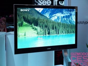
Sony OLED TV prototypeSony OLED TV prototype

The report also details the collaboration between Panasonic and Sony. The two companies have quite different technologies - Panasonic with its P-OLED and printing processes and Sony with small-molecules and VTE. It is claimed that Sony will mostly supply capital for Panasonic, and not technology. Sony's own OLED technology will be used though by Japan Display to make small sized panels.

Read the full story Posted: Sep 12,2012

Tailoring wettability results in better inkjet-printed electronics structures

Researchers from the Fontys University in The Netherlands have demonstrated that patterned plasma treatment of substrates gives them better control over inkjet printed structures (which results in higher quality printing).

The researches have used tailored wettability using InnoPhysics uPlasmaPrint technology that can locally change surfaces from hydrophilic to hydrophobic and vice-versa, creating patterns that make droplets spread in only one direction while restraining them in the other direction. Printed lines created in this way have both a very high homogeneity and a well-controlled width (without this technology the inkjet spreads in all directions which creates broader lines). In the research they used PixDro's LP-50 R&D inkjet printing platform.

Read the full story Posted: Sep 07,2012

Dupont at SID 2012

Dupont published some new OLED material specification, you can see them in the photo below. The lifetime (LT50) of their Blue fluorescent material is now over 33,000 hours (the the 0.14c0.13 blue, anyway) - which they say is good enough for OLED TVs. Their solution-processed materials are now more efficient than their evaporated-materials, but lifetime is probably lower (it's a bit hard to know since they only publish LT95 for those materials).

I had an interesting discussion with a Dupont employee involved in their OLED program. In January 2012 it was reported that the company is building a $30 million pilot production line for OLED TV displays using their new nozzle printing technology. It turns out that the report wasn't accurate - the facility that DuPont is building is a material production facility. They have no intention to start producing displays...

Read the full story Posted: Jun 18,2012 - 3 comments

Pioneer and Mitsubishi report advances in OLEDs made by web-coating, to expand current production capacity

Mitsubishi Chemical and Pioneer have jointly developed OLED elements produced using a wet coating process for the light-emitting layers. The two companies will establish a testing facility with an aim to commercialize this technology for OLED lighting mass production by 2014.

Mitsubishi's and Pioneer's OLED coating project began in January 2010, and in May 2011 the companies announced that they managed to fabricate a white OLED in which the emissive layer was formed in a coating process. That OLED featured 52 lm/W and a lifetime (LT50) of 20,000 hours (@1,000cd/m2 luminance). The new panel produced now features 56 lm/W and a lifetime (LT70) of 57,000 hours (@1,000cd/m2 luminance) which is quite an improvement.

Read the full story Posted: Jun 14,2012

UDC: green PHOLED adoption still ahead, confirms that Samsung is DuPont's Nozzle-printing licensee

Universal Display's management presented in an investor conference (Deutsche Bank's Clean Tech, Utilities and Power Conference). They gave an interesting introduction to the company and its business. In the Q&A, Sid Rosenblatt, the company's CFO says that currently their green PHOLED emitter is used in only two products: the Motorola Droid RAZR and the Sony Vita. This is set to change and they expect more products in the second half of 2012.

This explains why UDC's first quarter revenues were lower than expected - while red emitters sales were up 150% over last year, the green emitter sales have dropped, due to low Vita sales and high volume purchases in the previous quarter.

Read the full story Posted: May 15,2012

An interview with Merck's OLED unit VP, Dr. Udo Heider

Merck is a global pharmaceutical and chemical company based in Germany, working on high performance OLED materials. We're happy to post this third interview with Merck's OLED unit VP, Dr. Udo Heider:

Q: Dr. Heider, thanks for taking the time to do yet another interview with us.

Thanks Ron. I do appreciate this opportunity to communicate about our recent Merck OLED activities.

I'm assuming that Merck is still focused on Solution Processable materials. Can you give us a short update on the current status of your materials?

Yes, of course, we are very diligently focused on solution processable materials development based on our customers requests. As communicated in the past, Merck is working on solution processable small molecule materials. Our chemists have devised ways to redesign an evaporable small molecule and optimize its performance within a soluble device stack, applicable to the various soluble "printing" process windows.

Read the full story Posted: Apr 15,2012

On Sumitomo's OLED lighting program

Last week we reported that Sumitomo Chemical is planning to start mass producing OLED lighting panels later in 2012 based on their PLED technology in a ¥5-6 billion ($60-70 million) investement. Now Sumitomo finally announced that they plan to unveil panels at the L+B 2012 exhibition, and also unveiled a web page with lot's of info on their PLED lighting program. It seems that the company will commercial PLED panels for "decorative lighting" in 2013, and for general lighting in 2015.

In L+B2012 Sumitomo will show new PLED panels that are about 10 centimeters square each. There will be panels in sixty different colors, which are made using printing technology (all layers except the electrodes). The booth was designed by world-renowned Japanese lighting designer Motoko Ishii, with the theme The Colors of Japan The Colors of Harmony, in an innovative attempt to replicate—by means of lighting—the elegant and refined colors of ancient Japan in a modern day setting of a Japanese traditional tearoom. Here's what the booth will look like:

Read the full story Posted: Mar 25,2012

Sumitomo Chemical to start producing OLED lighting panels?

Update: Here's some official notice from Sumitomo on their PLED lighting plans...

There are reports that Sumitomo Chemical is planning to start mass producing OLED lighting panels. The company will start accepting orders next month, with mass production to begin later this year. Sumitomo will invest ¥5-6 billion ($60-70 million) in equipment.

Sumitomo will probably base their lighting panels on PLED materials. If indeed this report is true we'll probably hear something official soon.

Read the full story Posted: Mar 14,2012 - 1 comment

Konica Minolta developed a new high-accuracy printed electronics inkjet head

Konica Minolta has successfully developed a high-accuracy inkjet head capable of 1-picoliter drop size, the first for printed electronics applications. The new print head utlilizes the company's proprietary MEMS technologies for the first time. KM will start offering the new inkjet printhead (the KM128SNG-MB) in sample quantities by this spring.

The new print head is resistant to various inks required for industrial applications and suitable to use with low-viscosity inks. It can be used for all sorts of applications, including OLED display patterning and OLED lighting thin air coating.

Read the full story Posted: Feb 14,2012