OLED technology: introduction and basics
What is the OLED technology all about?
OLED panels are made from organic materials that emit light when electricity is applied through them. Since OLEDs do not require a backlight and filters (like LCD displays do), they are more efficient, simpler to make, and much thinner - and in fact can be made flexible and even rollable. OLED displays are used in TVs, smartphones, tablets, laptops, smartwatches and more.
OLEDs have a great picture quality - brilliant colors, infinite contrast, fast response rate and wide viewing angles. OLEDs can also be used to make OLED lighting - thin, efficient and without any bad metals.

You can read more about OLED displays their advantages in our OLED introduction page.
How do OLEDs work?
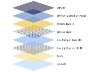
The main component in an OLED display is the OLED emitter - an organic (carbon-based) material that emits light when electricity is applied. The basic structure of an OLED is an emissive layer sandwiched between a cathode (which injects electrons) and an anode (which removes electrons).

OLED device structure
Modern OLED devices use many more layers in order to make them more efficient and durable, but the basic functionality remains the same.
An OLED panel itself is made from a substrate, backplane (electronics - the driver), frontplane (the organic materials and electrodes as explained above) and an encapsulation layer. OLEDs are very sensitive to oxygen and moisture and so the encapsulation layer is critical.
The substrate and backplane of an OLED display are similar to those of an LCD display, but the front plane deposition is unique to OLEDs. There are several ways to deposit and pattern the organic layers. Currently most OLED displays are made using vacuum evaporation, using a Shadow Mask (FMM, Fine Metal Mask) to pattern. This is a relatively simple method but it is inefficient (a lot of material is wasted) and very difficult to scale up to large substrates.
Some OLED materials are soluble, and these can be deposited using printing methods - mostly ink-jet printing. OLED makers hope that ink-jet printing may be a scalable, efficient and cheap way to deposit OLEDs. There is a next-generation OLED deposition technology referred to as maskless-production (usually based on photolithography) that seems to be of high interest.
AMOLED vs PMOLED
These terms relate to the driving method of the OLED display. A PMOLED (Passive-Matrix OLED) is limited in size and resolution (usually maximum resolution is around 128x128), but is cheaper and easier to make compared to an AMOLED (which uses an Active-Matrix). An AMOLED uses an active-matrix TFT array and storage capacitors. While these displays are more efficient and can be made large, they are also more complicated to make.
PMOLED displays are used in small devices or secondary displays while AMOLEDs are used in smartphones, smartwatches, tablets, laptops and TVs. Here's more information about the difference between PMOLED and AMOLED.
Challenges
The are still many challenges facing the OLED industry. Here's a list of some of the major ones:
- Material lifetime and efficiency (especially of the blue material)
- Soluble OLED material performance and production processes
- Better materials for flexible OLED and foldable ones
OLED technology today
OLED panels are being produced by several companies, led by Samsung Display, LG Display, BOE and others. around a billion OLED panels are produced annually (with capacity growing all the time), mostly for smartphones, TVs, wearables, IT devices and more. You can see a list of gadgets with OLEDs here.

Further reading
- Introduction to OLEDs
- OLED TV
- OLED lighting
- Flexible OLEDs
- Transparent OLEDs
- The OLED Toolbox, our comprehensive OLED information resource

